Πάνω σε μια νέα, μικρότερη και ταχύτερη RAM δουλεύουν αυτή τη στιγμή οι IBM και Micron που υπόσχεται ταχύτητα προσπέλασης 128Gbps ή με άλλα λόγια 10 φορές μεγαλύτερη από αυτήν που προσφέρουν οι τρέχουσες μνήμες!
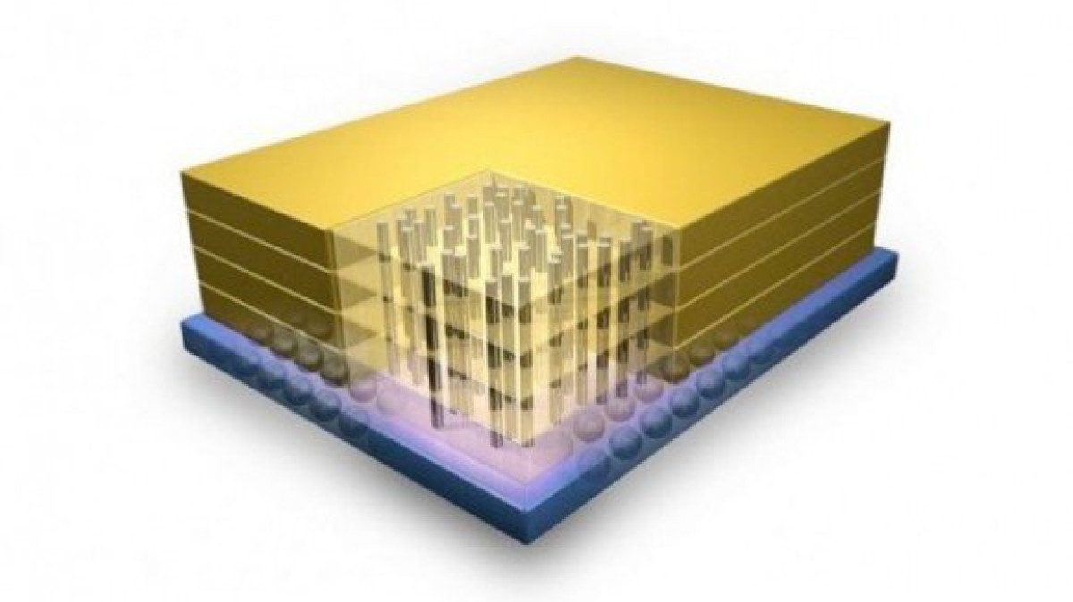
Η τεράστια ταχύτητα της νέας μνήμης οφείλεται τόσο στην τρισδιάστατη διάταξή της -τα μεμονωμένα τσιπς τοποθετούνται κάθετα και όχι το ένα δίπλα στο άλλο όπως στις σημερινές μνήμες- όσο και στα TSVs (Through-Silicon Vias) μέσω των οποίων επιτυγχάνονται οι επικοινωνίες.
Μεταξύ άλλων, οι δύο εταιρείες υποστηρίζουν ότι η τρισδιάστατη RAM έχει 70% χαμηλότερες απαιτήσεις σε ενέργεια από τις τρέχουσες μνήμες, ενώ ευελπιστούν ότι θα κυκλοφορήσει μέσα στα επόμενα δύο χρόνια. Ακολουθεί το επίσημο δελτίο τύπου της ΙΒΜ:
ARMONK, N.Y. & BOISE, Idaho - 01 Dec 2011: IBM (NYSE: IBM) and Micron Technology, Inc. announced today that Micron will begin production of a new memory device built using the first commercial CMOS manufacturing technology to employ through-silicon vias (TSVs). IBM's advanced TSV chip-making process enables Micron's Hybrid Memory Cube (HMC) to achieve speeds 15 times faster than today's technology.
Micron's Hybrid Memory Cube features a stack of individual chips connected by vertical pipelines or “vias,” shown above. IBM’s new 3-D manufacturing technology, used to connect the 3D micro structure, will be the foundation for commercial production of the new memory cube.
IBM will present the details of its TSV manufacturing breakthrough at the IEEE International Electron Devices Meeting on December 5 in Washington, DC.
HMC parts will be manufactured at IBM's advanced semiconductor fab in East Fishkill, N.Y., using the company's 32nm, high-K metal gate process technology.
HMC technology uses advanced TSVs — vertical conduits that electrically connect a stack of individual chips — to combine high-performance logic with Micron's state-of-the-art DRAM. HMC delivers bandwidth and efficiencies a leap beyond current device capabilities. HMC prototypes, for example, clock in with bandwidth of 128 gigabytes per second (GB/s). By comparison, current state-of-the-art devices deliver 12.8 GB/s. HMC also requires 70 percent less energy to transfer data while offering a small form factor — just 10 percent of the footprint of conventional memory.
HMC will enable a new generation of performance in applications ranging from large-scale networking and high-performance computing, to industrial automation and, eventually, consumer products.
"This is a milestone in the industry move to 3D semiconductor manufacturing," said Subu Iyer, IBM Fellow. "The manufacturing process we are rolling out will have applications beyond memory, enabling other industry segments as well. In the next few years, 3D chip technology will make its way into consumer products, and we can expect to see drastic improvements in battery life and functionality of devices."
"HMC is a game changer, finally giving architects a flexible memory solution that scales bandwidth while addressing power efficiency," said Robert Feurle, Vice President of DRAM Marketing for Micron. "Through collaboration with IBM, Micron will provide the industry's most capable memory offering."
[πηγή ibm]


